Advanced Process Control In Semiconductor Manufacturing

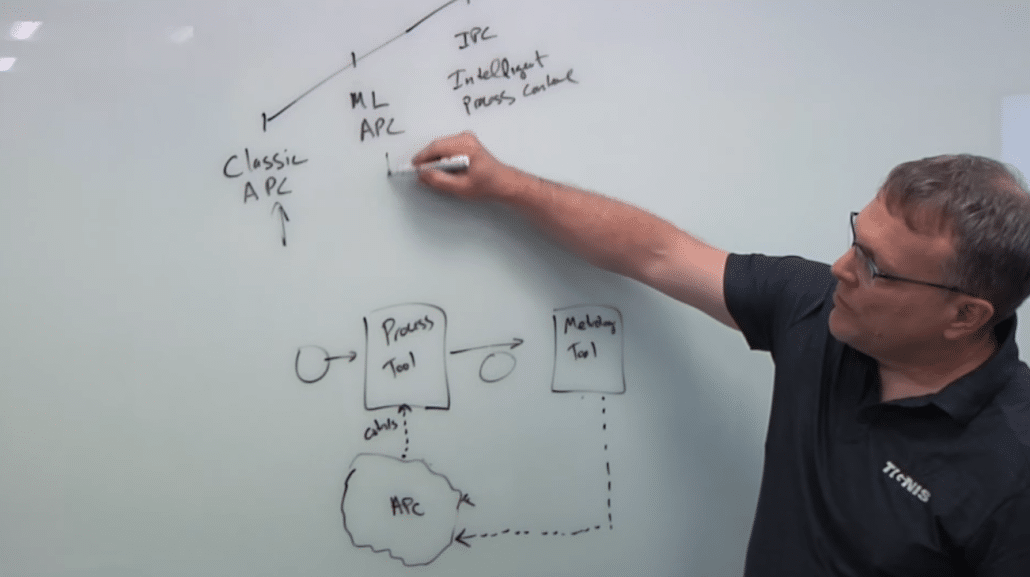
Advanced process control for semiconductor wafers is evolving in ways that can significantly improve yield and reduce scrap. As dimensions shrink, the need to improve manufacturing processes and reduce variability requires more precision. “Classic” APC was a step in the right direction, identifying problems in a process chamber, for example, and automating adjustments such as reducing electronic gases in a chamber or adjusting a wafer’s thickness due to critical dimension drift. That has been supplanted by machine learning-based APC, which adds virtual metrology to the picture. But there’s still a lot of data moving back and forth, which can result in multiple wafers being scrapped. Jon Herlocker, VP & General Manager of Tignis, A Cohu Analytics Solution, talks with Semiconductor Engineering about the next phase of APC, which includes intelligent process control, emulating the physics of an APC system, and optimizing it for multiple outcomes. This is part 5 of a 7-part series on AI in semiconductor manufacturing.


