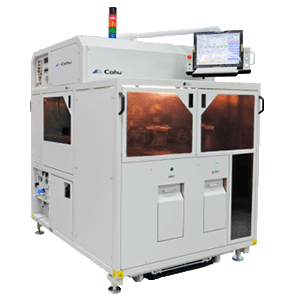
PAICe Inspection
Smarter Inspection. Higher Yield. Zero Compromise.

Live AI Decision to Improve Inspection Yield Without Throughput Compromise
Cohu’s PAICe Inspection™ is redefining optical inspection and metrology in semiconductor manufacturing environments. By integrating machine learning (ML) and deep learning algorithms into inspection workflows, manufacturers gain unparalleled accuracy, speed, and insight into their production processes. AI Inspection-based systems reduce overhead and improve manufacturing efficiency.


AI models are trained on thousands of labeled wafer and die images, enabling them to detect subtle, complex, or rare defects that traditional rule-based inspection might miss or misclassify. Distinguishes micro-cracks from scratches with infrared inspection, improving defect discernment and reducing misclassification.
This leads to fewer false negatives (missed defects), improved overall yield reliability and confidence in catching edge-case or evolving defect types.
AI Inspection doesn’t just detect anomalies – it classifies them. AI algorithms enable pattern recognition and precise defect classification and localization, reducing variability in manual tagging and increasing resolution for in-line decisions. Resulting in automated tagging of defect types (e.g., pattern shift, contamination, bridging), reduced reliance on manual review by engineers, and accelerated root cause analysis and yield learning.
With edge processing and AI-enabled decision-making, AI Inspection can process and analyze massive image datasets in real-time, reducing image transfer time, human-in-the-loop inspection bottlenecks and lot cycle time and bottlenecks in front-end or back-end lines.
Improved precision by rejecting fewer good dies or wafers that previously may have been flagged erroneously by overly conservative rule sets. This results in higher yields, better tool utilization, less unnecessary downstream handling and rework and improved customer trust in outgoing quality levels (OQL).
Unlike static rule-based systems, AI Inspection can be retrained or updated based on new defect types, process changes or technology nodes and line-specific variation. Deep learning automated root cause analysis improves defect traceability over time, allowing fab engineers to fine-tune processes and materials proactively. This enables adaptive inspection that evolves with your fab or OSAT environment.
AI Inspection naturally pairs with factory data systems and analytics platforms, enabling predictive correlations between inspection and test results, closed-loop feedback into process control, insightful dashboards for engineering and yield teams. A centralized database for fleet standardization toward Industry 4.0, helping unify inspection rules, tool performance metrics, and defect reporting across multiple fabs or lines.

Complete our contact form.